5. Implementation User’s Guide#
5.1. Introduction#
SpaceStudio provides two complementary workflows for transforming high-level system architectures into executable FPGA implementations: Architecture Implementation and FPGA-in-the-loop (FIL). These automated design flows bridge the gap between architectural specification and physical hardware deployment, supporting both traditional FPGA development cycles and rapid hardware-in-the-loop validation.
5.1.1. Architecture Implementation#
Architecture Implementation is the foundational workflow that transforms SpaceStudio designs into complete FPGA projects compatible with industry-standard Electronic Design Automation (EDA) tools. This comprehensive process performs design rule checking against target board constraints, maps all architectural components to vendor IP libraries or custom hardware blocks, synthesizes interconnect infrastructure, generates HDL entity declarations for modules and devices, cross-compiles embedded software for target processor architectures, configures toolchain options, links runtime libraries, and integrates operating system kernels with device drivers.
The Architecture Implementation workflow produces:
EDA project files: Complete Vivado or NanoXplore project hierarchies with all source files, constraints, and build scripts
RTL implementations: Synthesized or template HDL code for all hardware modules and devices
Software binaries: Cross-compiled application executables, drivers, and OS integration for embedded processors
Boot images: Bootloader configurations and filesystem images ready for deployment
This workflow is ideal for detailed design refinement, manual optimization, and scenarios requiring direct access to EDA tool flows for timing analysis, floorplanning, or bitstream post-processing.
5.1.2. FPGA-in-the-loop (FIL)#
FPGA-in-the-loop extends Architecture Implementation by automating the complete deployment and execution pipeline on physical FPGA hardware. FIL orchestrates the entire sequence from synthesis through on-hardware execution without manual intervention, enabling rapid design validation at full hardware speeds. The FIL workflow automatically performs bitstream generation, FPGA programming via JTAG, software deployment to the target board via SSH, application execution on embedded processors, and result capture back to the development environment.
The FIL workflow is optimized for:
Iterative design validation: Rapid testing of design changes on physical hardware
Performance profiling: Execution at full clock speeds with real-time I/O interactions
Hardware-software co-verification: Validating complete system behavior including actual peripheral interfaces
Continuous integration: Automated regression testing on physical FPGA boards as part of CI/CD pipelines
5.1.3. Workflow Selection#
Choose Architecture Implementation when you need:
Access to EDA tool project files for manual optimization or custom constraints
Bitstream generation for SD card-based deployment or standalone operation
Integration with third-party IP or custom build flows
Detailed timing analysis and floorplanning control
Choose FPGA-in-the-loop when you need:
Rapid design iteration with automated deployment to development boards
Performance validation on physical hardware without manual board configuration
Automated testing workflows integrated into development processes
Real-time execution profiling with actual I/O peripherals
Both workflows leverage the same core transformation engine but differ in their deployment and execution automation.
5.1.4. Supported Tools#
SpaceStudio supports the following EDA implementation tools:
Xilinx Vivado 2025.2
NanoXplore Impulse 24.3.0.0
Ensure the target EDA tool is properly installed, licensed, and configured on your development machine before initiating either workflow. SpaceStudio invokes the EDA toolchain programmatically to generate design files, perform synthesis, and execute place-and-route operations, requiring valid tool installations and accessible license servers. For FIL workflows, additional requirements include JTAG programming support and network connectivity to the target FPGA board.
5.1.5. General Considerations#
Menu Availability:
If no configured EDA tool supports the currently selected architecture (due to incompatible processor types, unsupported platform features, or missing tool configurations), the Architecture Implementation menu option (Tools → Architecture Implementation…) will be disabled (grayed out). Similarly, FIL launch configurations cannot be created for architectures without compatible EDA tool support.
Workflow Relationship:
FIL execution automatically invokes Architecture Implementation as a prerequisite step if the design has changed since the last implementation or if no previous implementation exists. This ensures the FPGA bitstream and software binaries are always synchronized with the current architecture state. You can also run Architecture Implementation independently to generate EDA project files without executing on hardware.
5.2. Design Preparation#
Before initiating Architecture Implementation, validate that your design conforms to the physical resource constraints and capabilities of the target FPGA board:
External Memory Controllers: Verify that the number of DDR/LPDDR memory controller instances does not exceed the memory interfaces available on the target FPGA board (e.g., most Zynq-7000 boards provide one DDR3 controller; Zynq UltraScale+ can support multiple DDR4 controllers).
External Memory Capacity: Ensure that configured external memory sizes do not exceed the physical DRAM capacity installed on the target board (check board documentation for installed memory size).
Block RAM (BRAM) Resources: Verify that the total BRAM requirements (sum of all
bramcomponent instances and embedded memories in IP blocks) do not exceed the BRAM resources available in the target FPGA device. Use FPGA Estimation to validate resource utilization.Clock Frequency Constraints: Ensure that system clock frequencies are within the range supported by the FPGA device’s speed grade and meet timing closure requirements. Consider that higher frequencies may fail timing analysis during implementation.
Some constraints can be validated within SpaceStudio using the Architecture Manager (see SpaceStudio documentation) or the FPGA Estimation tool (see section FPGA Estimation), which provides resource utilization analysis. Other constraints require manual verification against the target FPGA board’s technical datasheet and hardware specifications provided by the board vendor.
5.2.1. FPGA Estimation#
FPGA Estimation is an analytical tool within SpaceStudio that predicts hardware resource utilization for a given architecture configuration and target platform. This estimation accounts for logic resources (LUTs, flip-flops), memory blocks (BRAM, URAM), DSP slices, and I/O resources. Both available and consumed resources vary based on the target EDA toolchain (which affects synthesis optimization strategies), the specific FPGA device (which determines total available resources), and the selected speed grade.
Note
FPGA estimation is currently only supported for the Xilinx Vivado EDA.
- Click
This opens the FPGA Estimation configuration dialog shown below.
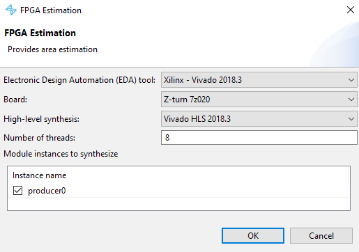
Figure 5.1 FPGA Estimation dialog#
Select the target EDA tool from the dropdown. If your preferred EDA tool is not listed, verify it has been properly configured in SpaceStudio preferences (refer to the General considerations section).
Select the target FPGA board platform from the available options for the chosen EDA tool.
Configure the number of concurrent estimations (thread count) to control parallelism during resource characterization. Higher thread counts accelerate estimation on multi-core systems.
In the HLS Options tab, select the HLS toolchain and designate which hardware-mapped modules should be synthesized through HLS to obtain accurate post-synthesis resource estimates (as opposed to behavioral estimates).
Click OK to initiate the estimation process.
FPGA resource estimation is performed by characterizing each hardware component within the architecture using vendor IP datasheets, synthesis databases, and optionally direct HLS synthesis. The initial characterization for a new EDA tool or board target may require significant time (potentially 15-30 minutes), as SpaceStudio builds a resource database by invoking the EDA tool to synthesize reference designs. Subsequent estimations leverage this cached characterization data for faster results. Monitor the console for any EDA tool errors during characterization, which may indicate improper tool configuration, missing IP licenses, or incompatible component-to-board mappings.
As shown in Figure 5.2, the results page displays estimated resource consumption compared to available resources on the target FPGA device. The comparison is broken down by resource type (e.g., Slice LUTs, LUT-RAM, Flip-Flops, BRAM tiles, DSP48 slices, URAM, I/O pins). Utilization percentages are calculated for each category, highlighting potential resource bottlenecks. Consult the FPGA device datasheet and board vendor documentation for detailed specifications on resource quantities and architectural characteristics.
Click the Details… button to view a component-level breakdown showing resource consumption for each module, device, interconnect, and IP block in the architecture. Advanced users can manually override resource estimates here for custom IP blocks. When finished reviewing results, click OK to close the estimation window and return to the main SpaceStudio interface.
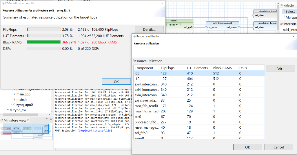
Figure 5.2 Results page for the estimation of FPGA hardware resources#
5.3. Architecture Implementation#
SpaceStudio automates the complete end-to-end architecture implementation workflow. When necessary, SpaceStudio orchestrates HLS tool invocation for hardware module synthesis, integrates the resulting RTL IP blocks into the system design, cross-compiles embedded software applications for target processor architectures, generates bus interface logic and protocol converters for inter-component communication, invokes EDA synthesis and implementation tools for bitstream generation, and provisions SpaceStudio-generated device drivers to interface the application software with operating system kernels and hardware peripherals.
- Click
This opens the Architecture Implementation configuration dialog shown below.
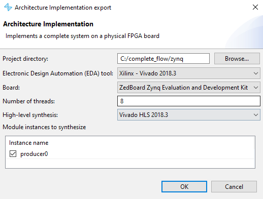
Figure 5.3 Architecture Implementation export dialog.#
Specify the implementation directory (referenced as
${arch_impl_dir}throughout this document). Due to operating system path length limitations (typically 260 characters on Windows, 4096 on Linux) and the deep directory hierarchy created by EDA tools, choose a directory close to the filesystem root (e.g.,/home/user/fpga_buildson Linux orC:\fpga_buildson Windows). SpaceStudio displays a warning if the path exceeds 100 characters, which may cause issues with nested EDA tool directories.Select the target EDA tool and target board platform from the dropdown menus.
Configure the number of concurrent synthesis jobs (thread count) to control parallelism during the build process. Higher thread counts reduce overall build time on multi-core systems but increase memory consumption.
In the HLS Options tab, select the HLS toolchain and enable checkboxes for hardware modules that should undergo automated HLS synthesis. Unchecked modules require manual RTL implementation, as described in Section 5.3.1.2.
Click OK to begin the implementation process. If the specified directory already exists, SpaceStudio prompts you to confirm deletion. Deleting the existing directory is recommended to ensure a clean build and avoid stale file conflicts.
Architecture Implementation begins executing the multi-stage build process, which can be time-intensive. Typical implementation times range from 10 to 45 minutes, though complex designs with many hardware modules, extensive interconnect hierarchies, or aggressive timing constraints may require significantly longer (up to several hours). The dominant time factor is the EDA tool’s synthesis, place-and-route, and timing closure iterations. Monitor the build console for progress updates through each stage: HLS synthesis, RTL generation, software cross-compilation, IP integration, design synthesis, implementation, and bitstream generation. Successful completion is indicated by the message Project Implementation [Completed successfully.] in the SpaceStudio console. If errors occur, SpaceStudio provides diagnostic messages identifying the failure point. For assistance interpreting error messages or resolving build failures, consult the SpaceStudio documentation or contact Space Codesign Systems technical support.
File |
Description |
|---|---|
create_project_hook.tcl |
Tcl script sourced at the end of the generated EDA project creation script. The script must define a spacestudio_create_project_hook proc, which is called right after being sourced, while the project is still open. |
5.3.1. Board bring-up#
5.3.1.1. EDA synthesis conditions#
During the Architecture Implementation workflow, SpaceStudio analyzes the design to determine whether fully automated bitstream generation can proceed without requiring manual HDL intervention. Automated EDA synthesis and bitstream generation execute when the following conditions are satisfied:
No custom device implementations required: All device instances are either standard library IP blocks or have their “Only used for simulation” flag enabled (see Figure 5.4), indicating they are not part of the physical implementation.
All hardware modules use HLS synthesis: Every module instance mapped to hardware has been selected for automated HLS synthesis, with no modules requiring manual RTL implementation.
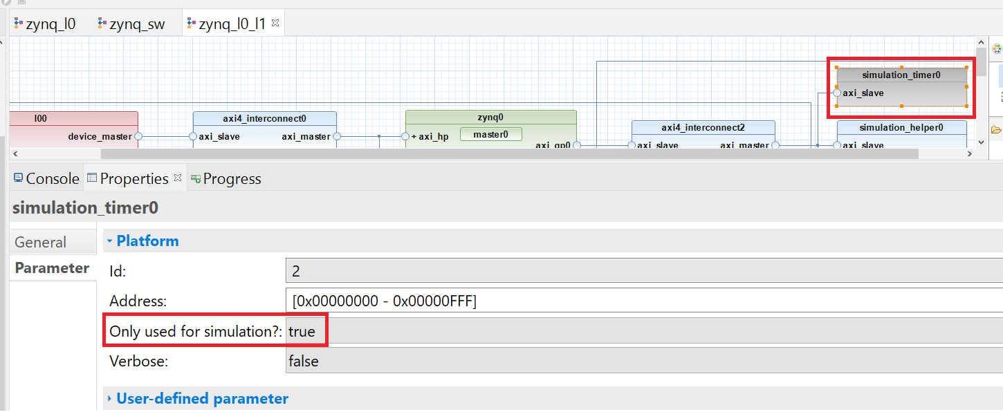
Figure 5.4 “Only used for simulation” flag for device instances#
When these conditions are not met, SpaceStudio halts after generating the EDA project structure and creating template HDL files, allowing you to manually implement the required RTL code for custom modules and devices (detailed in section Section 5.3.1.2). In this semi-automated mode, you must manually complete subsequent steps including HDL implementation, EDA synthesis invocation, bitstream generation, and boot image creation—tasks that would otherwise be handled automatically by SpaceStudio in the fully automated flow. Future SpaceStudio releases may provide enhanced automation for these manual implementation scenarios.
5.3.1.2. User-provided module/device implementation#
Note
This feature is not supported for NanoXplore targets.
As described in Section 5.3.1.1, you can designate specific components for manual RTL implementation rather than automated HLS synthesis. For these components, Architecture Implementation generates IP wrapper infrastructure, establishes all necessary interconnect connections to integrate the component into the overall system, and creates a template VHDL entity file containing the required port interface definitions. The remainder of the system (interconnects, processors, standard IP blocks, HLS-synthesized modules) is generated and integrated normally.
To complete manual implementation, open the generated template VHDL file and implement the component’s behavioral architecture. For Vivado-based designs, the template file is located at:
${arch_impl_dir}/application_repository/core/${component}/src/${component}.vhd
Where ${component} is the instance name of the module or device requiring implementation.
For detailed guidance on implementing component architectures, including interface protocol requirements and timing constraints, consult the Implementing Hardware Components documentation.
5.4. FPGA-in-the-loop (FIL)#
FPGA-in-the-loop (FIL) is an advanced execution mode that enables automated deployment and execution of SpaceStudio designs directly on physical FPGA hardware. Unlike traditional FPGA workflows that require manual bitstream programming, SD card preparation, and board configuration, FIL automates the entire deployment pipeline—from bitstream generation through on-board execution—providing a seamless hardware-in-the-loop testing environment for validating designs at full hardware speed with real I/O interfaces.
5.4.1. Overview#
FIL execution bridges the gap between simulation and physical deployment by automating the complete hardware bring-up sequence. When you launch a FIL execution, SpaceStudio:
Synthesizes the design: Invokes the EDA toolchain to perform RTL synthesis, place-and-route, and bitstream generation for the target FPGA device.
Programs the FPGA: Automatically transfers the bitstream to the target board via JTAG and configures the FPGA fabric with your custom hardware design.
Deploys software: Transfers cross-compiled application binaries and SpaceStudio-generated drivers to the embedded Linux filesystem on the target processor via SSH/SCP.
Executes the application: Launches the embedded software application on the target processor cores, allowing hardware-software co-execution on real hardware.
Captures results: Streams console output, performance metrics, and application results back to the SpaceStudio development environment for analysis.
This automation eliminates manual board configuration steps, accelerates design iteration cycles, and enables continuous integration workflows for FPGA-based designs.
5.4.2. Prerequisites#
FIL execution requires specific hardware, software, and network infrastructure:
Hardware Requirements:
A supported FPGA development board (e.g., Xilinx Zynq-7000 ZedBoard, Zynq UltraScale+ ZCU102, or compatible platforms)
The board must include an embedded processor capable of running Linux (typically ARM Cortex-A cores)
JTAG programming interface
Network connectivity (Ethernet port or equivalent) for SSH communication
Software Requirements:
Embedded Linux operating system configured and running on the target processor
SSH server (OpenSSH) running on the target with public key authentication enabled
Properly configured EDA tools (Vivado, Vitis) with valid licenses on the host development machine
Network Configuration:
The host development machine and target FPGA board must be connected to the same IP network subnet
Static IP address assignment recommended for the target board to ensure consistent connectivity
SSH public key authentication configured (passwordless login) for automated file transfer
Firewall rules allowing SSH (port 22) and JTAG communication
SpaceStudio Configuration:
FIL execution is configured through launch configurations, as described in the User Guide under the FIL configuration section. Key configuration parameters include:
Host IP address: The IP address of the development machine reachable from the target board
SSH credentials: Path to the SSH private key for passwordless authentication to the target
JTAG cable: The JTAG interface identifier for programming the FPGA
5.4.3. Execution Workflow#
To execute a design using FIL:
Configure the architecture: Ensure your architecture includes a processor instance running embedded Linux with network support enabled and SSH public key provisioning configured (see User Guide for Linux configuration details).
Create a FIL launch configuration: Right-click the architecture in the Project Explorer, select Run As → Run Configurations…, create a new Execute on FPGA configuration, and configure the FIL parameters (board selection, HLS options, execution timeout, host IP, SSH key path).
Launch FIL execution: Click Run to initiate the automated workflow. SpaceStudio will:
Perform Architecture Implementation (if not already completed or if design has changed)
Invoke EDA synthesis to generate the FPGA bitstream
Program the FPGA fabric via JTAG
Transfer application binaries and drivers to the target via SCP
Execute the application on the embedded processor
Stream console output back to SpaceStudio
Monitor execution: Observe application output in the SpaceStudio console view. The console displays both kernel messages and application output from the embedded Linux system.
Analyze results: Upon completion, review execution logs, performance data, and any generated output files. The application terminates either by calling the appropriate shutdown function or when the configured wall-clock timeout expires.
5.4.4. Benefits of FIL#
Accelerated Design Validation: FIL eliminates the manual overhead of SD card preparation, bitstream transfer, and board reconfiguration, reducing iteration time from minutes to seconds for incremental design changes.
Hardware-Speed Execution: Unlike simulation, which can be orders of magnitude slower than real-time, FIL executes designs at full hardware clock frequencies, enabling realistic performance profiling and timing validation.
Real I/O Testing: FIL allows testing with actual hardware peripherals (ADCs, sensors, communication interfaces) connected to the FPGA board, validating interface timing and signal integrity that cannot be accurately modeled in simulation.
Continuous Integration: The automated nature of FIL enables integration into CI/CD pipelines, allowing automated regression testing of FPGA designs on physical hardware as part of the development workflow.
Co-debugging: FIL supports debugging workflows where GDB connects to the target board for source-level debugging of embedded software while hardware executes in the FPGA fabric.